

High-Complexity
Hardware
From Silicon to Qualified Product
Team with proven experience in integrated photonics, deep sub-micron ASICs (FinFET), world-class scientific instrumentation, AI hardware, and quantum technologies — from chip to product in the market.
140+
Engineers
100–400Gbps
Module speed
<12nm FinFET
ASIC technology node
Tens of thousands
Devices manufactured
30+
Products Developed
What we do
Our Business Units
Three specialized business units, one integrated platform — from coherent photonics to custom chips.
R&D Photonics
We develop photonic devices for telecom, data centers, and AI — from PIC design (Integrated Photonics) to qualified module.
- ›Silicon Photonics (SiPh) — Receivers, Modulators, Passives
- ›Tunable Lasers (thousands of units manufactured)
- ›Coherent Modules: CFP2-DCO, QSFP-DD, OSFP
- ›Optical Amplifiers (EDFA and Raman)
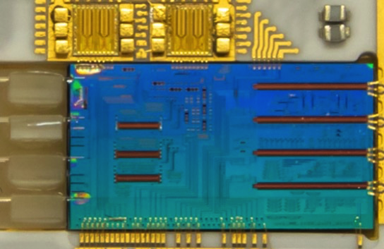
Product Engineering
We turn concepts into advanced hardware products — with full development flow, pilot lines, and local manufacturing.
- ›Packaging: flip-chip, wirebonding, hermetic sealing
- ›Class 1000 Clean Room + SMT 140k CPH
- ›Testing: HALT, Telcordia GR-468, JEDEC, IPC
- ›X-ray Detectors (9.4 MP, 2000 FPS, vacuum)
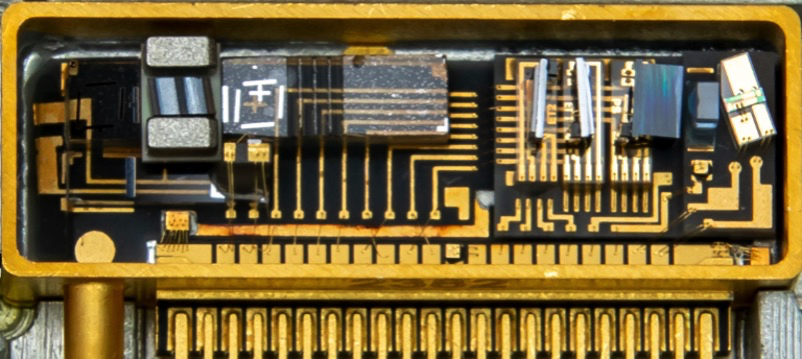
ASIC Design
Custom chip design — from RTL to tapeout in deep sub-micron, with full flow: frontend, backend, analog, and silicon validation.
- ›FinFET experience (TSMC) — 1.0B+ transistors
- ›DSP-ASIC 60 GBd DP-16QAM (400Gbps)
- ›Team of specialized ASIC engineers
- ›Digital, Analog, DFT, UVM Verification
Markets
Strategic Applications
Optical & Quantum Communications
Optical transport networks, DCI, metro, and long-haul
- 400Gbps OIF-compliant
- CFP2-DCO, QSFP-DD, OSFP modules
- External cavity tunable lasers
- Silicon photonics transceivers (100/200G)
Data Center & AI
High-speed interconnects for AI clusters and hyperscale
- 400G optical I/O and beyond
- Silicon photonics for AI accelerators
- Low-power coherent DSP ASICs
- Integrated transceiver modules
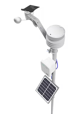
Instrumentation & IoT
Advanced sensors, scientific instrumentation, and industrial connectivity
- PIMEGA — 9.4 MP X-ray detector for synchrotrons
- LWS300/NBS300 — IoT sensor platform for facilities management
- NIMBUS — Satellite environmental telemetry
- DBD — Urban mobility NFC/EMV/QR
Results
By the Numbers
1.0B+
ASIC Gate Count
140+
Group Engineers
400G+
Module Speed
6nm
FinFET Technology
Ecosystem
Partnerships & Collaborations
Grupo HwIT


Industrial Partnerships


Academic Ecosystem


Get in Touch
Contact Us
Have an advanced hardware project? Our technical team evaluates feasibility.
Our Facilities
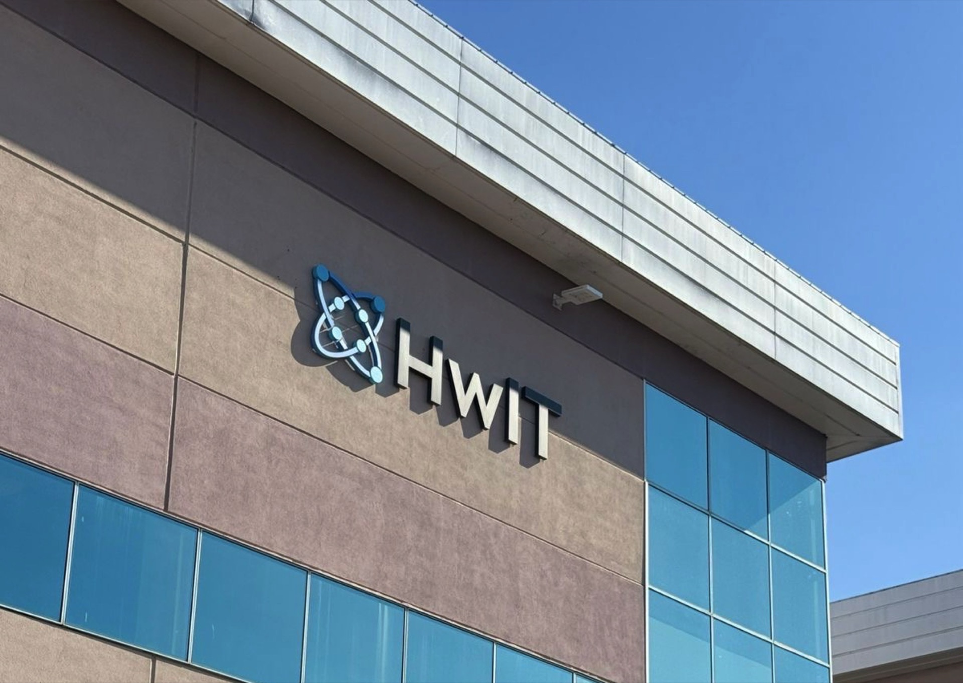
Campinas / SP, Brazil
HQ + Lab + Clean Room
Av. Cambacicas, 610 — 2,500 m²
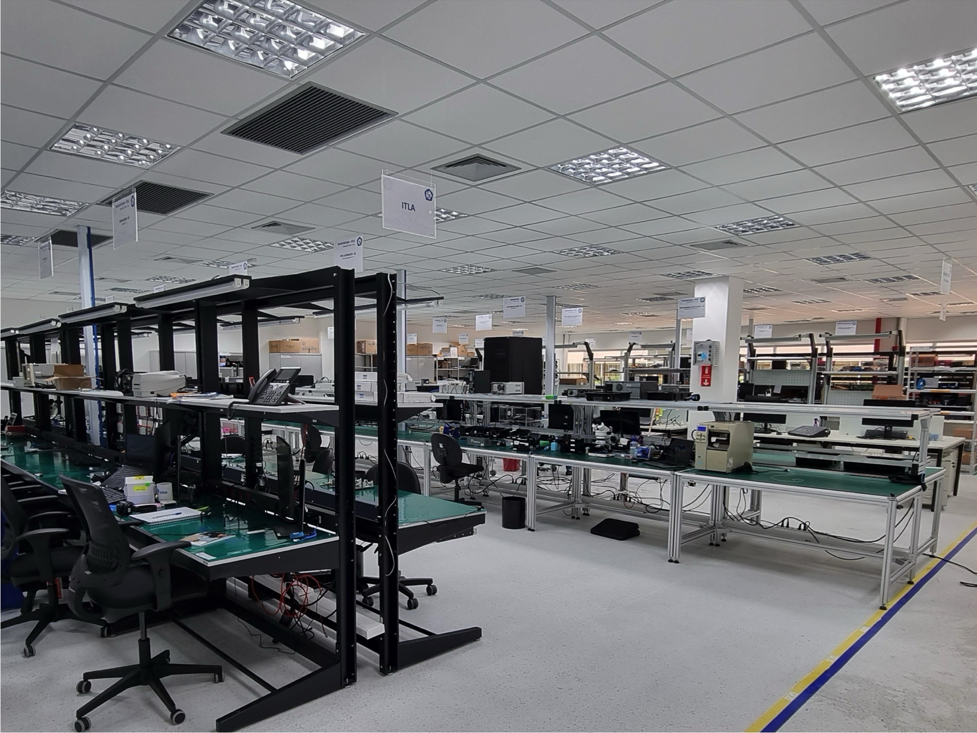
Paulínia / SP, Brazil
SMT Manufacturing — 140k CPH
R. Jose Moreira de Souza, 184 — 700 m²
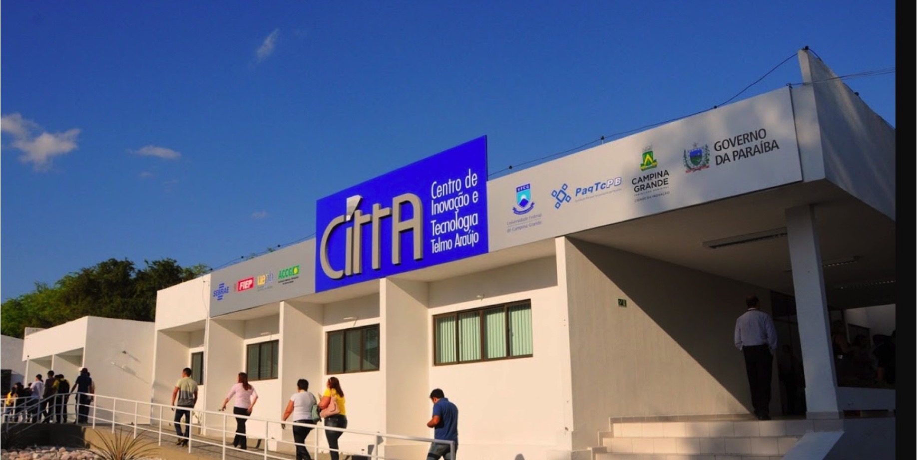
Campina Grande / PB, Brazil
ASIC & Photonics Design
R. Aprígio Veloso, 1500 — 100 m²